Semiconductor Technology
Optoelectronics
We focus on the design and characterization of advanced materials and architectures for photodetectors, radiation detectors, photovoltaic (PV) devices, and transparent conducting oxides (TCOs). The work aims to develop high-performance, stable, and lead-free materials that enable efficient light–matter interaction and charge transport. By combining experimental and computational approaches, the research explores the structure–property relationships governing optical absorption, carrier dynamics, and radiation response—paving the way for next-generation optoelectronic systems for energy harvesting and sensing applications.
Faculty: Dr. Sebin Devasia (Click here)
Nanophotonic Materials and Devices
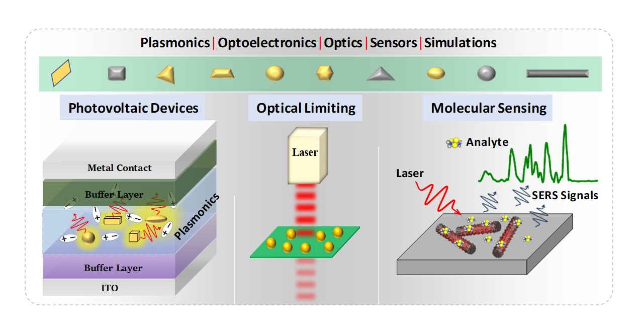
How do we manipulate light interaction with matter at the sub-wavelength scale? This question lies at the core of modern physics, where controlling light-matter interactions beyond the diffraction limit has the potential to revolutionize optoelectronic devices. Precise control of light at nanoscale can be attained with the proper utilization of distinct properties of plasmonic and semiconductor nanostructures. Nanophotonic Materials and Devices (NMD) laboratory mainly focuses on the design and development of various sizes and shapes of metal and semiconductor nanostructures using physical vapor deposition and chemical synthesis methods. These nanostructures are engineered to efficiently control the light-matter interaction for advanced optical and optoelectronic applications, pushing the boundaries of photo-energy harvesting, molecular sensing, and nonlinear optics.
Faculty: Dr. Abhijith T (Click here)
RAM/EMI shielding materials
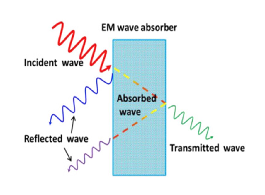
EMI shielding is a technique of creating a barrier that prevents leakage of strong electromagnetic fields that are interfering with military equipment. Objective of the work is to develop a composite that improves and withstands high temperatures and EMI shielding applications in harsh environments. In our group we develop Bn and ceramic oxide based Emi shielding/RAM materials.
Faculty: Dr. Anuradha M Ashok (Click here)
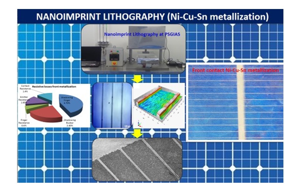
Silver-less (Ni-Cu-Sn) Narrow-Line Width Front Contact Metallization Patterns for Solar Cells
Screen printing dominates solar cell metallization due to high throughput but faces challenges from high silver usage, shadow loss, and interruptions in narrow finger lines. At PSGIAS, we developed cost-effective, silver-free fine-line front contact metallization using nanoimprint lithography (NIL) and maskless lithography. An in-house NIL tool was built for integration with crystalline silicon solar cell fabrication. Finite Element Analysis (FEA) guided optimized grid designs, enabling ~1% efficiency improvement by reducing shading loss. Replacing silver with Ni/Cu/Sn metallization offers similar conductivity at lower cost. This approach enables scalable fabrication of fine-line (<20 μm) grids, significantly reducing solar cell manufacturing costs.
Faculty: Dr. P Biji (Click here)
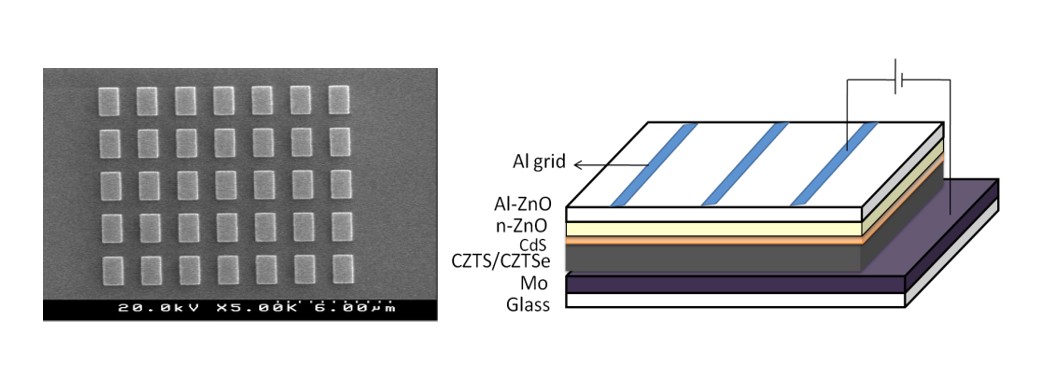
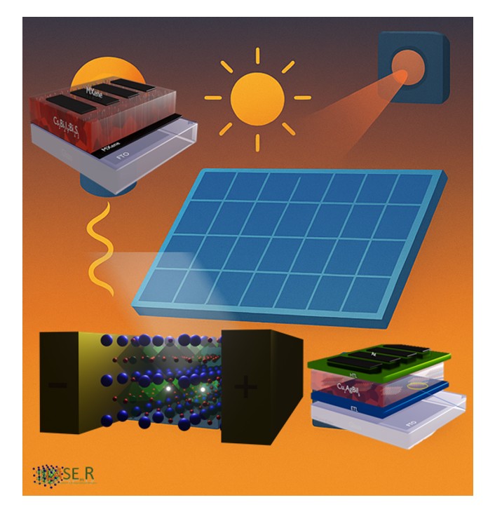
Thin film solar cells
Today’s thin film photovoltaic technologies rely on elements that are costly and rare in the earth’s crust (e.g. In, Ga, Te) and are toxic (e.g. Cd). Hence, in future cost reduction and increased production, using abundantly available non-toxic elements, seem to be the main issues. Cu2ZnSnS4 (CZTS), having the kesterite structure, is one of the most promising absorber layer candidates for low cost thin film solar cells. Thin film solar cell device with the CZTS as active layer and micro-structured back contact layer were fabricated and analysed.
Faculty: Dr. Anuradha M Ashok (Click here)
Computational Materials
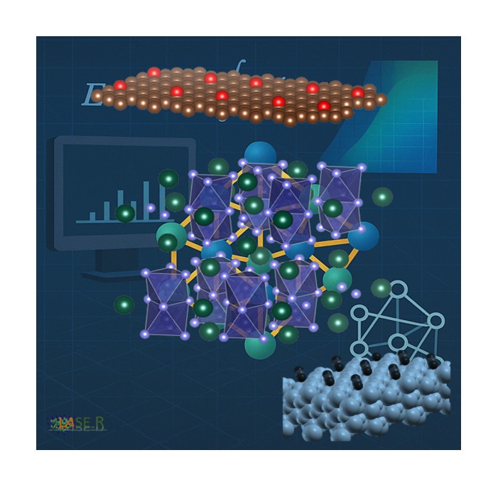
Computational materials research, integrating Density Functional Theory (DFT) calculations, machine learning (ML), and Monte Carlo simulations to design and understand advanced functional materials. DFT is employed to investigate structural, electronic, and optical properties for applications in photovoltaics, sensors, and energy devices. ML methods are developed and applied to accelerate materials discovery and predict key properties such as bandgap, thermal stability, and defect energetics. Additionally, Monte Carlo simulations are used to model matter–radiation interactions, enabling insights into radiation response and damage mechanisms in semiconductors and nanomaterials.
Faculty: Dr. Sebin Devasia (Click here)
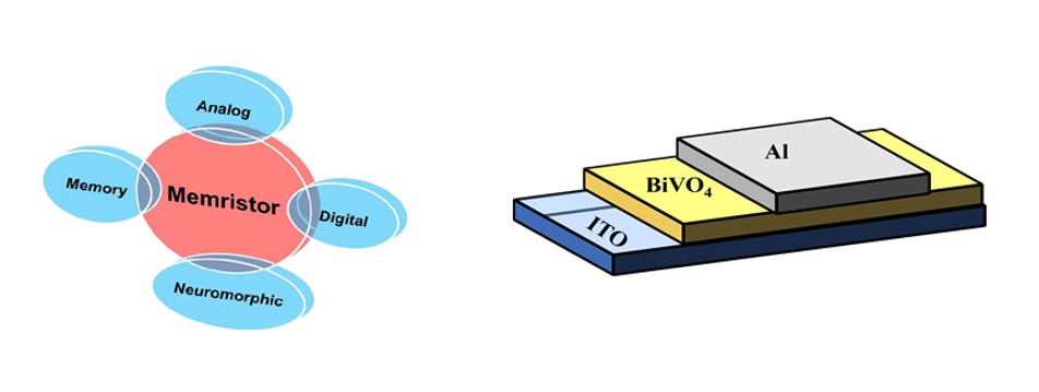
Memristors
Memristors (memory + resistor) are an emerging field among researchers and it is considered as fourth passive electronic component followed by Inductors, Capacitors, and Resistors. Our group is working on inorganic complex oxide type material having suitable narrow band gap. Memristor devices are fabricated with semiconductor oxide nanomaterials as active layer between metal contacts by a simple cost-effective method.
Faculty: Dr. Anuradha M Ashok (Click here)